![]()
Das Kompetenznetz Funktionelle
Nanostrukturen wurde gefördert
durch die
Baden-Württemberg Stiftung.
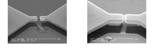
Electron micrographs of Au nanowires after transport measurements. In the left graph the wire is clearly distorted, although the mask is well defined. In the right example the narrow slit in the mask defining the nanowire is stuffed, but a metal wire on the substrate clearly exists with a resistance R ~ 8 Ohms
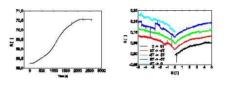
Resistance as a function of time for the sample similar to that shown in the figure above (left). The sample was inserted into the cryostat at t = 0 s. The leveling-off of the resistance signals that the sample arrives at base temperature (~ 4.5 K). The right panel displays magneto resistance measurements taken at 4.5 K. The individual traces are shifted vertically by 0.04 W for clarity. The zero-field resistance R0 = 70.5 Ohms has been subtracted.
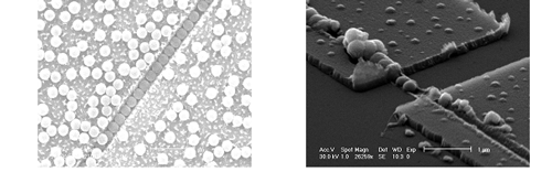
Left: Electron micrograph of a colloid chain in a SiO 2 trench. The
diameter of the spheres is 270 nm and the depth of the trench is 150 nm.
Right: After the second lithography step defining the contact leads.
Two spheres were accidentally removed from the trench upon lift-off.