![]()
Das Kompetenznetz Funktionelle
Nanostrukturen wurde gefördert
durch die
Baden-Württemberg Stiftung.
Optical microscopy of an Au surface after illumination with 3 beam pulsed laser interference at the wavelength 532 nm. The strong gradients of the laser illumination pattern lead to lateral material transport. Lateral spacing of the dots is 1mm.
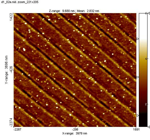
Atomic force microscopy of a self assembled monolayer (SAM) on Silicon after two beam pulsed laser interference at the wavelength 266 nm. The SAM has been locally removed, thus surface energies can modified locally. Period of the lines is 400nm.
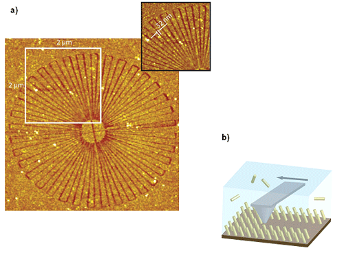
(a) This is a topographic AFM image of a structure written into a silane self-assembled monolayer (SAM), which was prepared directly on top of a polished silicon wafer. The topographic contrast of about 2 nm is due to the AFM-tip induced removal of monolayer within the »written« lines. The process is schematically depicted in (b). Within the lines of the pattern the hydrophilic silicon oxide surface is accessible.
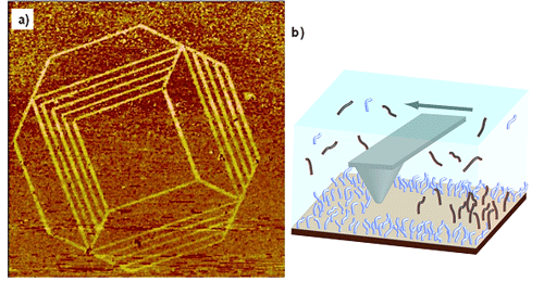
(a) This is a tapping mode phase image of a structure written into a polymer brush layer. The 0.5 nm thick layer, was replaced by a layer of another polymer. The contrast in the phase image which was taken after the samples were dried at ambient conditions, reveals a high contrast in the tip sample interaction between the elastomeric and the glassy polymer layer. A schematic representation of the structuring process is depicted in (b).
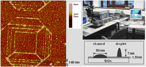
Dewetting pattern of a polymer film on a pre-patterned substrate. The polymer wets preferentially the AFM-structured portions of the surface and forms narrow channels with a width of about 80 nm. The excess material within in the unstructured background forms small (50 nm diameter) droplets with a relatively high contact angle. Our home-built structuring system is shown in the upper right. A scheme of the cross section of a channel and a droplet is shown in the lower right.